
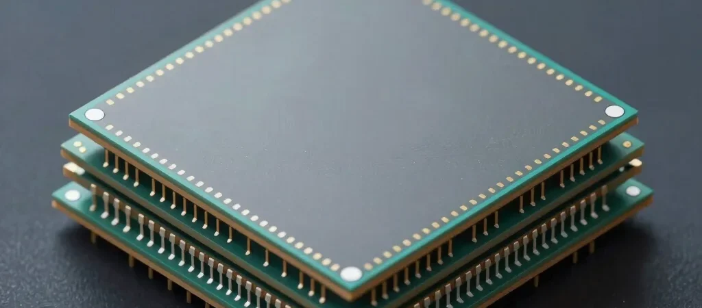
The semiconductor industry has reached a structural limit where shrinking individual transistors on a single silicon die yields diminishing economic and physical returns. In response, leading foundries are pivoting away from monolithic fabrication toward heterogeneous chiplet architectures bound by high-density interconnects. This architectural shift enables engineers to combine specialized functional blocks fabricated on different process nodes into a single integrated system.
Stacking Architectures and Thermal Management
Vertical three-dimensional packaging allows memory and logic tiles to sit directly atop one another, dramatically shortening electrical trace lengths and reducing interconnect latency. However, placing high-power compute dies in close vertical proximity creates intense thermal density challenges that demand microchannel liquid cooling solutions. Advanced thermal interface materials are now critical enablers for maintaining structural integrity under sustained operational loads.
Optical Interconnects and Future Data Transfer
Replacing traditional copper interconnects with integrated silicon photonics marks the next major evolutionary step for server backplanes. By converting electrical signals into optical pulses directly on the package, data throughput expands by multiples while power dissipation drops substantially. Early commercial implementations in hyper-scale data centers demonstrate that optical chiplets will power the next generation of high-performance computing clusters.